 |
KBTEM-OMO – Joint Stock Company
Advanced optical based solutions for photomask and wafer patterning, automated inspection and mask repair |

KBTEM-OMO Joint Stock Company (“KBTEM-OMO” JSC) started its activity in 1962 as an optical-mechanical equipment division of KBTEM (Design Office for Precision Electronic Engineering). December, 16, 1991 in accordance with the order of the Ministry of Industry of the Republic of Belarus #82, Scientific and Production Republican Unitary Enterprise KBTEM-OMO was set up with a legal entity status as part of the State Scientific and Production Corporation for Precision Engineering Planar. From 2011 KBTEM-OMO is officially acknowledged as Scientific Institution by the State Committee on Science and Technology of the Republic of Belarus and National Academy of Science of Belarus. January 23, 2014 the Republican Unitary Scientific and Production Enterprise KBTEM-OMO was transformed into a Joint Stock Company «KBTEM-OMO» («KBTEM-OMO» JSC).
The main line of activity of KBTEM-OMO is the scientific and technological development as well as production of special opto-mechanical, process, inspection and measurement equipment.
| Equipment For Direct Writing |
Pattern generators are considered to be complex tools in manufacturing of semiconductor devices. High requirements to such equipment can be met only with the help of high-end technology.
KBTEM-OMO has extensive experience in the development of opto-mechanical equipment. The model line of multichannel laser pattern generators for microelectronics built on the raster scan concept is characterized by exceptional functional features:
- direct writing on wafers (maskless optical lithography);
- overlay option;
- high throughput;
- process switch to mask writing mode.
The universality of such high-performance equipment makes it indispensable for scientific institutions and microelectronics manufacturers.
 |
EM-5389 MULTICHANNEL LASER PATTERN GENERATOR
Pattern generators provide possibility for pattern writing on semiconductor substrates with simultaneous previous layers alignment (maskless optical lithography). The patterning is based on a raster scanning principle.
|
||||||||||||
 |
EM-5289B MULTICHANNEL LASER PATTERN GENERATOR
Pattern generators provide possibility for pattern writing on semiconductor substrates with simultaneous previous layers alignment (maskless optical lithography). The patterning is based on a raster scanning principle.
|
||||||||||||
 |
EM-5189-02 MULTICHANNEL LASER PATTERN GENERATOR
Pattern generators provide possibility for pattern writing on semiconductor substrates with simultaneous previous layers alignment (maskless optical lithography). The patterning is based on a raster scanning principle. The EМ-5189-02 exposure system uses a continuous ultraviolet semiconductor laser with optical pumping at 355nm wavelength. Laser output power: 250 mW.
|
| Tools For Proximity Exposure and Double-Side Lithography |
EM-5026xx series and EM-5096 tools are intended for pattern alignment on photomasks and wafers (substrates) and further transfer of this pattern from mask to wafer through contact (proximity) exposure of wafer photoresistive layer.
Main features:
– wedge compensation and wafer thickness compensation without contact with the photomask;
– 3 coordinates (X, Y, Q) high precision wafer manipulator with coarse and fine alignment modes;
– ability to handle 0.2 mm to 0.8 mm wafers made of fragile materials (GaAs, LiNbO3) and rectangular substrates;
– built-in vibration protection unit;
– energy saving mode.

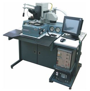
EМ-5026АМ MASK ALIGNER EM-5026AM system is designed to align the photomask pattern with the wafer (substrate) pattern and to transfer the pattern from the photomask onto the wafer (substrate) through contact (proximity) exposure of the wafer photoresist layer. EM-5026AM features the following automatic systems: |
Specifications
*Subject to customer requirements |
||||||||||||||||||||||||||

EM-5096 MASK ALIGNER EM-5096 system is designed to align the photomask pattern and the wafer pattern and to transfer the pattern from the photomask onto the wafer through the contact (proximity) exposure of the wafer photoresist layer. EM-5096 features the following automatic systems: Double field microscope with smooth magnification adjustment. Loading-unloading of wafers and substrates onto the chuck is performed by the operator manually. |
Specifications
*Subject to customer requirements |
||||||||||||||||||||||||||

EM-5026M1 MASK ALIGNER EM-5026M1 system is designed to align the photomask pattern with the wafer (substrate) pattern and to transfer the pattern from the photomask onto the wafer through contact (proximity) exposure of the wafer (substrate) photoresist layer. EM-5026M1 features the following automatic systems: Single field microscope with smooth magnification adjustment. Loading-unloading of wafers and substrates onto the chuck is performed by the operator manually. |
Specifications
*Subject to customer requirements |
||||||||||||||||||||||||||

EМ-5026B DOUBLE-SIDE MASK ALIGNER The EM-5026B system is designed to perform a contact (proximity) exposure of the top (front) side of a wafer or a substrate through alignment of the photomask pattern with the pattern on the bottom (back) side of the wafer or substrate. EM-5026B features the following automatic systems: Semiautomatic wafer loading/unloading. |
Specifications
*Subject to customer requirements |
||||||||||||||||||||||||||

EM-5186 DOUBLE-SIDE ALIGNMENT MARK PLACEMENT SYSTEM The EM-5186 system is designed for mark placement on the bottom side of the wafer (substrate). The mark is aligned with alignment marks on the top side of the wafer (substrate). The system allows to manufacture double side lithography wafers (substrates) with traditional lithography equipment. The tool can be used for manufacturing of semiconductor devices, hydrid, optical, optoelectronic and other devices, MEMS, MOEMS. EM-5186 allows to form marks on transparent substrates. |
Specifications
*Subject to customer requirements |
||||||||||||||||||||||||||
Click here for further information.
